
Three frames you can check by eye: an SPI byte, an I2C write, and a UART character. Each drawing uses equal time slots so the bit order is obvious. A chip datasheet still has to supply the nanosecond limits. These figures do not.
SPI mode 0, master sends 0xA5
Mode 0 means the clock idles low (CPOL = 0) and the bit is sampled on the rising edge (CPHA = 0). CS is active low. While CS is low there are eight rising edges. MOSI is 10100101, which is 0xA5 with the most significant bit first. MISO is 00111100, which is 0x3C, sampled on the same edges.
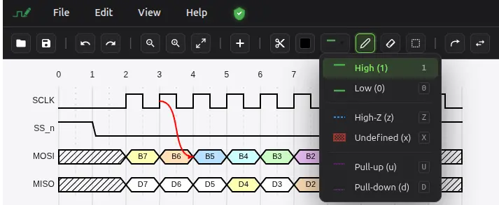
Modes 1, 2, and 3 move the idle level of the clock or the sampling edge. The SPI guide lists CPOL and CPHA for all four. The names tSETUP, tHOLD, tCLK, tCSS, and tCSH are the ones a peripheral datasheet will number.
I2C write of 0x0F to address 0x50
I2C uses two open-drain wires, SCL and SDA, both idle high. A start condition is SDA falling while SCL is high. After that, each bit is stable while SCL is high and may change only while SCL is low. The address 0x50 is the seven bits 1010000. The following 0 is the write bit. The peripheral pulls SDA low for one clock to acknowledge. The data byte 0x0F follows, most significant bit first (00001111), and a second acknowledge ends the byte. A stop condition is SDA rising while SCL is high.

Standard-mode I2C (100 kHz) and Fast-mode (400 kHz) specify different minimums for start hold, data setup, and stop setup. The I2C guide lists those names and the usual values from the I2C specification. Clock stretching, which this frame does not show, is the peripheral holding SCL low to ask for more time.
UART 8N1 character 0x55
A UART frame has no shared clock. The line idles high. A start bit forces it low for one bit time. The data bits follow, least significant bit first. 0x55 is 01010101, so the wire carries 1, 0, 1, 0, 1, 0, 1, 0 after the start bit. 8N1 means eight data bits, no parity, and one stop bit. The stop bit returns the line high. The next start bit is another falling edge.

The bit time is 1/baud. At 115200 baud it is about 8.68 µs. The drawing does not scale that interval. It only shows the order: idle, start, eight data bits, stop.
Redraw any of these
Open the editor, add a bit row per wire, and paint the levels from the figure. The handbook shows how to add arrows and export PNG or SVG for a note or a datasheet.